Physical Vapor Deposition - also known as PVD Coating - refers to a variety of thin film deposition techniques where solid metal is vaporized in a high vacuum environment and deposited on electrically conductive materials as a pure metal or alloy coating.
As a process that transfers the coating material on a single atom or molecule level, it can provide extremely pure and high performance coatings which for many applications are much preferable to electroplating. PVD Coating processes are an environmentally friendly process that can greatly reduce the amount of toxic substances that must be disposed of with more conventional types of coating that involve fluid precursors and chemical reactions.
At the heart of every microchip and semiconductor device, PVD Coatings enable the solar panel industry to make greener electricity as well as surgical and medical implants that require the highest degrees of purity. It produces coatings with superior hardness, durability and resistance to wear. PVD Coatings reduce friction for high performance moving parts making them widely used in the aerospace and automotive industry, and for cutting tools where long lasting durability is the crucial success factor.
PVD is fundamentally a vacuum coating technique vaporizing a metal to a plasma of atoms or molecules and depositing them on a wide range of substrates. Carried out in a high vacuum chamber approximating outer space at 10-2 to 10-4 millibar, the process usually takes place between 150 and 500 Degrees C.
The material to be coated is secured in a fixture and placed in the vacuum deposition equipment chamber. The equipment is pumped down to the optimum pressure depending upon the coating materials, substrate and process used, and the object to be coated is often preheated and sputter cleaned.
A wide variety of types of PVD coatings are available, including Zirconium Nitride (ZrN), Zirconium Carbon Nitride (ZrCN), Titanium Nitride (TiN), Titanium Carbon Nitride (TiCN), Chromium Nitride (CrN), Chromium Carbon Nitride (CrCN), and Chromium Nitride (CrN).
The carbides, nitrides, silicides and borides that make up the PVD coating materials each have special qualities tailored to specific applications. Graphite and titanium for example are often used in high performance aerospace and automotive component where friction and temperature are crucial success factors.
To achieve a uniform thin film coating thicknesses that are often a few atoms or molecules thick, parts to be coated are often rotated on several axis at a uniform speed, or placed on conveyor belts moving past the deposition material’s plasma stream. Single or multi-layered coatings can be applied during the same deposition cycle.
Additionally, reactive gasses such as nitrogen, oxygen or acetylene are introduced into the vacuum deposition chamber to produce a very strong bond between the coating and substrate when it’s deposited. Although the thin film coatings are only a few microns thick, they form an extremely adherent coating with high lubricity lowering friction and heat that makes PVD the perfect choice for high performance cutting tools and engine parts.
Physical Vapor Deposition Coatings are also highly resistant to tarnishing and corrosion enabling them to be used for a wide range of decorative finishes with colors that do not fade. PVD produces highly brilliant finishes that make watches highly resistant to scratches and scrapes, and is used in a wide variety of optical applications ranging from glasses to self-cleaning tinted windows. Their resistance to corrosion makes them widely used on household items such as door handles, plumbing fixtures and marine fixtures.
Report on Y2O3 Coating:
Y2O3 coating on inner surface of quartz tube OD=25.4mm, ID=22mm
The coating was examined by the following methods:
Surface morphology by HRSEM (High Resolution)
EDS analysis on the inner surface (Carbon coating for the analysis)
Metallographic cross-section (SEM Philips XL-30)
The results were as follows:
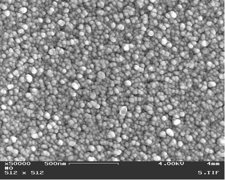
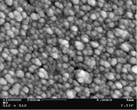
The surface morphology is shown in Figs 1, 2 and reveals dense coating of nano-sized crystals (~30nm)
In Fig 2 is the same as in Fig 1 at the higher magnification. The particle size is ~30nm
No pin-holes were revealed.
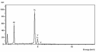
EDS (LINK ISIS) spectrum obtained in the middle of the tube is shown in Fig 3 and reveals 88wt% Y2O3+ 12wt% SiO2 (substrate)
Since the depth of EDS analysis is ~ 1µm, there is the indication that Y2O3 layer thickness is close to 1µm
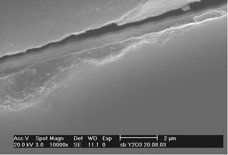
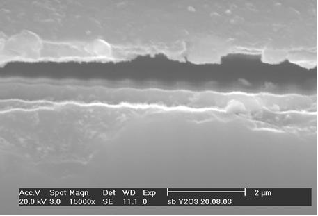
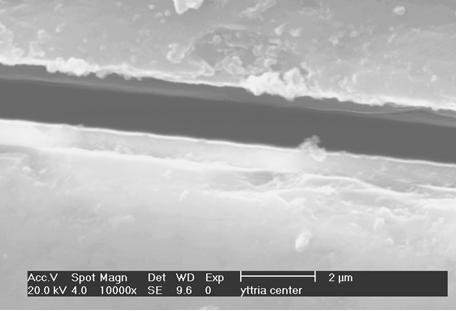
Metallographic cross-section prepared at the end of the tube reveals dense, uniform coating of ~0.5µm - see arrows in Figs 4 and 5
No discontinuities or other defects were revealed at the quartz/Y2O3 layer interface
In the central part of the tube a coating thickness of ~0.75µm was observed, see Fig 6
